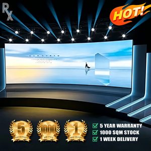
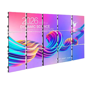
CE Certified Mini LED Screen Manufacturer & Exporter
Engineering Whitepaper & Strategic Global Procurement Guide: High-Reliability Flip-Chip COB, Ultra-Fine Pitch Architectures, and Zero-Standby Intelligent Power Infrastructure.
375k+
SQM Delivered Globally
500+
Years Engineering Heritage
14+
Patented Breakthroughs
100%
Factory FAT Tested
Precision Display Portfolios
Engineered Commercial & Industrial Mini LED Systems
Custom-engineered visual solutions compliant with CE EN 55032 Class B EMC and EN 62368-1 electrical safety directives. Built for 24/7 mission-critical operations, DOOH infrastructures, and premium corporate presentation spaces.
Mini LED Chip-on-Board (COB) vs. Conventional SMD Architecture
A deep-dive technical comparison for specifiers, systems integrators, and procurement officers evaluating lifecycle thermal stability, MTBF, pixel failure rates, and optical dispersion.
Thermal Dissipation & Die Bonding
Traditional Surface Mount Devices (SMD) rely on dual-tier leadframes that act as thermal insulators, generating high junction temperatures (Tj > 85°C) at micro pitches. Mini LED COB directly attaches flip-chip dies onto multi-layer FR4/metal-core substrates, lowering thermal resistance (θjc) by over 45% and mitigating blue-shift degradation.
Fine-pitch SMDs are notoriously prone to edge impact, pixel shearing, and oxidation from airborne pollutants. Our CE-certified Mini LED panels feature vacuum-applied optical epoxy encapsulation, shielding diodes to achieve IP54/IP65 surface ratings against moisture, ESD surges (>8kV), and dust accumulation.
Surface hardness rated ≥4H for wipe-clean maintenance
Zero solder joint fracturing under vibrational loading
Optical Uniformity & Contrast Dynamics
By pairing microscopic flip-chips with nano-scale black matrix encapsulation, Mini LED achieves a static contrast ratio of up to 20,000:1. The matte anti-glare finish removes the typical moiré patterns common in broadcast recording and virtual production stages while broadening viewing angles to 170° horizontal and vertical.
Wide color gamut spanning 98% DCI-P3 coverage
16-bit to 22-bit grayscale depth without low-light clipping
Combining UK engineering governance, strict on-floor Factory Acceptance Testing (FAT), and dedicated regional Pixel Depots to guarantee uninterrupted operational longevity.
Independent Engineering by Design
Rather than relying on generic contract assembly, our proprietary intellectual property governs every module, driver layout, and cabinet chassis. We partner with specialized manufacturing lines, deploying resident engineers to enforce strict quality benchmarks.
In-Person Factory Acceptance (FAT)
Every batch undergoes stringent 72-hour burn-in tests, high-temperature soak chambers, thermal imaging analysis, and full chromaticity binning before packing. No screen ships until signed off by our dedicated quality assurance engineers.
Zero-Standby Energy Management
Compatible with patented intelligent power control systems (such as digiLED ZEUS®), enabling large-format video walls to drop to true 0.0W standby consumption during off-hours, significantly cutting operating expenses and ESG carbon footprints.
Regional Pixel Depots (UK & USA)
Our localized service centers in Las Vegas and the United Kingdom house dedicated module calibrators, microscope wire bonders, and emergency buffer stock to provide same-week turnarounds for critical display components.
Full CE, EMC & Low Voltage Compliance
Fully compliant with the European Union's 2014/30/EU (EMC Directive) and 2014/35/EU (LVD Directive). Engineered with multi-stage EMI filtration, shielded interconnects, and flame-retardant structural polymers (UL94-V0).
Consultant & Integrator Centric Support
We work directly with AV consultants, structural engineers, architects, and media agencies to deliver custom structural load calculations, power distribution design, and precision mechanical drawings tailored to site constraints.
Market Forecasting & Strategic Roadmap
Future Procurement Trends in Mini LED Display Infrastructure
Key technological, commercial, and regulatory shifts shaping commercial display investments over the next 5 to 7 years.
Trend 01
Shift toward MIP (Micro-in-Package) & Hybrid COB
While standard COB leads ultra-fine pitch display walls, MIP technology is achieving significant volume scaling. By separating the testing of microscopic pixel packages prior to surface placement, production yields climb to >99.5%, bringing sub-1.0mm resolutions closer to traditional P1.5 SMD price points.
Trend 02
Carbon Border Adjustments & Eco-Directives
European public tenders and enterprise procurement workflows increasingly factor in the EU Ecodesign Directive Lot 5/9 and the Carbon Border Adjustment Mechanism (CBAM). Displays that eliminate idle thermal dissipation and incorporate intelligent sleep states gain priority in competitive bidding.
Trend 03
Native AV-over-IP & Direct SMPTE ST 2110
Future control architecture bypasses conventional external receiving cards and DVI/HDMI convertor boxes. Mini LED cabinets now embed direct 10Gb/25Gb fiber interfaces capable of decoding uncompressed SMPTE ST 2110 broadcast streams directly at the panel processor.
Trend 04
Dynamic Common Cathode Architectures
Procurement specifications now frequently mandate Common Cathode IC driver topography. By delivering independent voltage rails for red (2.8V) and blue/green (3.8V) chips, overall heat generation drops by up to 30%, noticeably extending the operating lifespan of the LED matrix.
Technological Vectors
Emerging Engineering Horizons in Micro-Pitch Mini LED Systems
Explore the engineering advances driving high-frame-rate rendering, optical clarity, and structural longevity across professional broadcast, simulation, and mission-critical visualization.
High Frame Rate (HFR) & Low Latency Processing
Virtual production stages and broadcast studios require display driver refresh rates exceeding 7680Hz with frame multipliers supporting up to 240fps. Mini LED display engines now incorporate customized PWM scan drivers to eliminate camera scanline artifacts and phase-angle flicker during rapid tracking camera moves.
Ultra-low latency pipeline (≤ 1 frame end-to-end)
Genlock phase-offset tuning with ±5ns sync tolerance
Active-Matrix (AM) Substrate Convergence
Traditional passive matrix (PM) time-multiplexed scanning faces physical limits in current delivery and power density below P0.7mm. Next-generation Mini LED systems are adopting glass-based thin-film transistor (TFT) active-matrix drives, where individual sub-pixels maintain dedicated continuous driving currents, reducing peak voltage spikes and electromagnetic emissions.
True continuous illumination without multiplex flicker
Flat mechanical tolerances with glass thermal stability
Rec.2020 Spectral Purity & Quantum Dot Color
Through the integration of colloidal quantum dot (QD) color conversion layers deposited directly over monochromatic blue Mini LED chips, new display matrices expand their spectral emission purity. This delivers up to 90% coverage of the demanding BT.2020 wide color gamut while retaining deep, stable blacks under ambient gallery light.
Narrower spectral FWHM (Full Width at Half Maximum)
Enhanced ambient contrast with anti-reflective optical coatings
Procurement & Engineering Due Diligence
Frequently Asked Technical & Commercial Questions
Practical insights for purchasing managers, electrical engineers, and commercial display project specifiers.
What specific standards must a Mini LED screen pass to achieve authentic CE Certification?
Authentic CE compliance requires full verification against two primary directives: the Electromagnetic Compatibility Directive (2014/30/EU) under EN 55032 (Emissions for multimedia equipment, ideally Class B for commercial/residential deployment) and EN 55035 (Immunity), along with the Low Voltage Directive (2014/35/EU) under EN 62368-1 (Audio/video, information and communication technology equipment safety). Our products undergo certified testing by accredited third-party laboratories with full test reports and Declarations of Conformity (DoC) provided for specifier submittals.
How does Mini LED Chip-on-Board (COB) solve the on-site pixel damage common in rental and high-traffic spaces?
In conventional SMD screens, each individual pixel package is soldered via pins to the PCB surface. Any accidental impact or cleaning friction can dislodge or shear these packages. COB encapsulates the microscopic LED dies within a continuous, cured optical resin layer that bonds directly with the PCB substrate. This creates a smooth, robust surface rated up to 4H hardness that resists impacts, allows direct wipe-down cleaning, and prevents moisture and dust from reaching the underlying circuitry.
What is the optimal viewing distance formula for fine-pitch Mini LED screens?
The industry benchmark for the visual acuity threshold (where individual pixels resolve into a smooth image) is approximately 1.0 meter of distance per 1.0mm of pixel pitch. For example, a P1.25 Mini LED display achieves retina-like visual coherence at approximately 1.25 meters (4 feet). For executive conference rooms and control centers with close viewing parameters (1.5m - 2.5m), a pixel pitch between P0.9mm and P1.5mm provides crisp text rendering and sharp detail without noticeable pixel structure.
How do you handle color and brightness consistency across different manufacturing batches?
We maintain strict single-bin wavelength and forward-voltage sorting directly at the wafer level. For every major enterprise project, we preserve an additional 10% to 15% spare module buffer drawn from the exact same wafer production run. Furthermore, our control system architecture stores per-pixel radiometric calibration data in on-module EEPROM, ensuring that replaced modules match the screen's chromaticity within a 2-step MacAdam ellipse.
What power management features are implemented to reduce thermal load and energy waste?
Our systems use dynamic common-cathode driver topologies, which supply dedicated lower voltages directly to the red dies, reducing heat generation by up to 30% compared to standard common-anode systems. Additionally, they are engineered for compatibility with patented zero-standby power controllers (such as digiLED ZEUS®), enabling large displays to power down to 0.0W during non-operational hours, avoiding unnecessary standby draw and extending the operating lifespan of the power supplies.
What after-sales service and depot repair support do you provide internationally?
We support our global installations through dedicated regional Pixel Depots located in the UK and Las Vegas, USA. These facilities are staffed by factory-trained calibration engineers and equipped with microscopic precision rework tools, wire bonders, and spectral profiling cameras. This setup allows local component-level repairs and module re-calibration without the delays and risks associated with shipping sensitive display panels internationally.
Plan Your Enterprise Mini LED Installation with Our Engineering Team
Whether you require technical submittals for architectural review, customized DWG framing schematics, CE certification dossiers, or exact viewing-distance pixel calculations, our team is ready to assist your project from concept through commissioning.
 Conference / Corporate