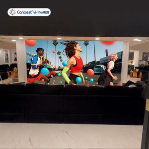
From optical resin-encapsulated fine-pitch matrices to structural floor tiles engineered for heavy traffic, explore our field-certified hardware deployed across international stadiums, retail flagships, and critical control centers.

In modern solid-state visual installations, standard Surface Mounted Diode (SMD) configurations display vulnerability to physical shear forces, humidity egress, and electrostatic discharge (ESD). While Chip-on-Board (COB) mounts unencapsulated dies directly to the PCB to achieve pitch densities below 1.2mm, its complex repairability and substantial initial capital outlay limit its deployment in commercial rental, interactive floors, and high-traffic retail.
Glue-on-Board (GOB) technology serves as an engineered bridge. GOB applies a patented optical-grade polyurethane or epoxy nanocomposite over an automated SMD assembly. This protective layer cures into an optically clear, void-free shield that increases solder-joint shear resistance from a baseline 1.5 kgf to exceeding 12.0 kgf, completely mitigating pixel dropout caused by accidental collisions, cleaning implements, or public physical engagement.
A frequent issue in poorly fabricated GOB displays is optical refraction shift and chromatic deviation. Professional manufacturing mandates that the potting resin maintain a refractive index matched closely to the LED mold compound (n ≈ 1.52–1.54). In addition, high thermal conductivity (k > 1.2 W/m·K) within the polymer blend accelerates heat flux from the semiconductor junction through the thermal vias of the printed circuit board, preventing uneven thermal throttling and blue-shift degradation over continuous operational cycles.
Certified IK08 to IK10 mechanical impact ratings. Resists blunt tool impact and pedestrian kinetic pressure up to 2,000 kg/m².
Complete hermetic seal rated IP65/IP68 front-face. Eliminates moisture penetration, sulfurization, and salt-spray copper track corrosion.
Nano-matte chemical surface treatments eliminate specular glare while maintaining native 160° horizontal and vertical viewing cones.
Provides an electrostatic barrier rated up to 15kV air discharge, eliminating high-voltage circuit damage in dry, carpeted interiors.
Procurement workflows for institutional LED display installations are shifting from baseline cost-per-square-meter calculations to rigorous total-cost-of-ownership (TCO) assessments. Over an operational lifecycle of 50,000 to 100,000 hours, servicing unprotected SMD modules in public, high-traffic spaces frequently incurs cumulative maintenance costs equal to or exceeding initial capital acquisition.
As corporate control hubs, broadcast suites, and simulation environments adopt pixel pitches between P0.9 and P1.5, traditional SMD configurations experience elevated failure rates from physical interactions during routine cleaning and maintenance. GOB nano-encapsulation eliminates these failure vectors, providing mission-critical installations with structural protection comparable to industrial flat panels while retaining the modular serviceability and bezel-free continuity of LED video walls.
Global ESG directives and rising commercial energy costs have elevated active and passive power consumption into primary technical selection criteria. Traditional large-format displays draw significant power even when idle. Modern engineering integrates hardware-level power management, such as the globally patented digiLED ZEUS® architecture, which completely eliminates standby energy draw, lowering carbon footprints and helping facilities meet net-zero compliance targets.
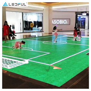
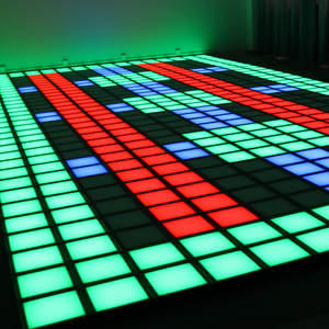
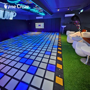
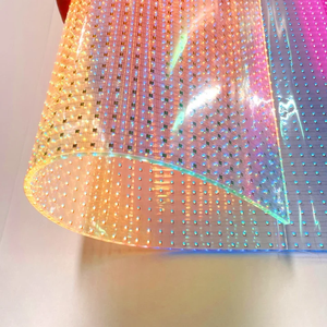
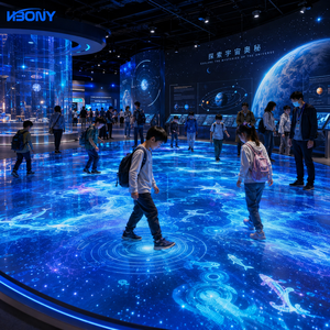
Interactive gaming hubs, broadcast environments, and retail flagship stores increasingly deploy dynamic load-bearing GOB floors and optically clear film displays. High-density capacitive and optical radar sensor arrays embedded beneath transparent GOB structures support sub-15ms touch latencies, transforming functional architecture into responsive data interfaces that support high-impact commercial engagement.
We do not operate as a single-factory assembly line. We engineer custom display hardware to proprietary IP specifications and manage complete, hands-on production oversight across elite fabrication facilities.
Rather than standardizing on fixed catalog hardware, our engineers assess project-specific viewing geometries, structural constraints, and duty cycles. We partner with elite fabrication hubs, specifying our own printed circuit boards, driver ICs, and encapsulation resins to build each display to precise project requirements.
digiLED engineers remain on the factory floor throughout production cycles. Every cabinet undergoes thermal aging, colorimetric uniformity validation, and strict Factory Acceptance Testing (FAT) before palletization, ensuring zero-fault site handoffs.
With regional Pixel Depots operating out of Las Vegas, USA, and Hertfordshire, United Kingdom, we stock batch-matched LED diodes, processing controllers, and custom power supplies. Our clients receive responsive, multi-decade post-warranty servicing rather than short-term product obsolescence.
Objective engineering answers for procurement committees, consultants, and AV systems integrators evaluating display protection technologies.
Submit your mechanical drawings, environmental conditions, and pixel-pitch specifications. Our engineering team will produce an end-to-end structural, optical, and thermal plan tailored to your project.